
1. Introduction to Microcontroller:
A microprocessor system consists of a microprocessor with memory, input ports and output ports connected to it externally. A microcontroller is a single chip containing a microprocessor, memory, input ports and output ports. Since all four blocks reside on the one chip, a microcontroller is much faster than a microprocessor system.
We have several other basic microcontroller families such as PIC, M68HCXX, and AVR etc. All these basic microcontrollers are useful for implementing basic interfacing and control mechanisms for simple applications. There are several applications which require lot of computation and high speed data processing. In such applications advanced microcontrollers and microprocessors are used. One such advanced architecture is ARM.
1.2 History of ARM:
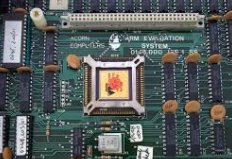
ARM stands for Advanced RISC machine. The first processor in ARM family was developed at Acorn Computers Ltd between October 1983 and April 1985. Acorn Computers was a British computer company established in Cambridge, England, in 1978. The company worked for Reduced Instruction Set Computer (RISC) processor design. The company produced a variety of computers which were very popular in the United Kingdom. These included the Acorn Electron, the BBC Micro and the Acorn Archimedes. Particularly BBC Micro computer dominated the UK educational computer market during the 1980s and early 1990s.
1.3 ARM Architecture:
The ARM core uses RISC architecture. Its design philosophy is aimed at delivering simple but powerful instructions that execute within a single cycle at a high clock speed. The RISC philosophy concentrates on reducing the complexity of instructions performed by the hardware because it is easier to provide greater flexibility and
intelligence in software rather than hardware. As, a result RISC design plays greater demands on the compiler. In contrast, the traditional complex instruction set computer (CISC) relies more on the hardware for instruction functionality, AND consequently the CISC instructions are more complicated.
Certain design features have been characteristic of most RISC processors:
One cycle execution time: RISC processors have a CPI (clock per instruction) of one cycle. This is due to the optimization of each instruction on the CPU. Each instruction is of a fixed length to allow the pipeline to fetch future instructions before decoding the current instruction.
Pipelining: The processing of instructions is broken down into smaller units that can be executed in parallel by pipelines. Ideally the pipeline advances by one step on each cycle for maximum throughput. Instructions can be decoded in one pipeline stage.
Large number of registers: The RISC design philosophy generally incorporates a larger number of registers to prevent large amount of interactions with memory. Any register can contain either data or an address. Registers act as the fast local memory store for all data processing operation.
Load-store architecture: The processor operates on data held in registers. Separate load and store instructions transfer data between the register bank and external memory.
These design rules allow a RISC processor to be simpler, and thus the core can operate at higher clock frequencies.
Difference between RISC and CISC architectures:
CISC RISC
|
1. |
Complex instructions taking multiple cycles |
Simple instructions taking one cycle |
|
2. |
Any instruction may refer to memory |
Only LOAD/STORE refer to memory |
|
3. |
Not pipelined or less pipelined |
Highly pipelined |
|
4. |
Instructions interpreted by the micro-program |
Instructions executed by the hardware |
|
5. |
Variable format |
Fixed format instructions |
|
6. |
Many instructions and modes |
Few instructions and modes |
|
7. |
Complexity in the micro-program |
Complexity in the compiler |
|
8. |
Single register set |
Multiple register sets |
ARM Processor Core:
Similar to most RISC machines ARM works on load-store architecture, so only load and store instructions perform memory operations and all other arithmetic and logical operations are only performed on processor registers. The figure shows the ARM core data flow model. In which the ARM core as functional units connected by data buses,. And the arrows represent the flow of data, the lines represent the buses, and boxes represent either an operation unit or a storage area. The figure shows not only the flow of data but also the abstract components that make up an ARM core.
- Data enters the processor core through the Data bus. The data may be an instruction to execute or a data item. This ARM core represents the Von Neumann implementation of the ARM data items and instructions share the same bus. In contrast, Harvard implementations of the ARM use two different buses.
- The instruction decoder translates instructions before they are executed. Each instruction executed belongs to a particular instruction set.
The ARM processors, like all RISC processors, use load-store architecture. This means it has two instruction types for transferring data in and out of the processor: load instructions copy data from memory to registers in the core, and conversely the store instructions copy data from registers to memory. There are no data processing instructions that directly manipulate data in memory. Thus, data processing is carried out solely in registers.
Data items are placed in the register file – a storage bank made up of 32-bit registers. Since the ARM core is a 32- bit processor, most instructions treat the registers as holding signed or unsigned 32-bit values. The sign extend hardware converts signed 8-bit and 16-bit numbers to 32-bit values as they are read from memory and placed in a register.
The ALU (arithmetic logic unit) or MAC (multiply – accumulate unit) takes the register values Rn and Rm from the A and B buses and computes a result. Data processing instructions write the result in Rd directly to the register file. Load and store instructions use the ALU to generate an address to be held in the address register and broadcast on the Address bus.
One important feature of the ARM is that register Rm alternatively can be preprocessed in the barrel shifter before it enters the ALU. Together the barrel shifter and ALU can calculate a wide range of expressions and addresses.
After passing through the functional units, the result in Rd is written back to the register file using the Result bus. For load and store instructions the incrementer updates the address register before the core reads or writes the next register value from or to the next sequential memory location. The processor continues executing instructions until an exception or interrupt changes the normal execution flow.
ARM Bus Technology:
Embedded systems use different bus technologies. The Peripheral Component Interconnect (PCI) bus connects devices such as video card and disk controllers to the X 86 processor buses. This is called External or off chip bus technology.
Embedded devices use an on-chip bus that is internal to the chip and allows different peripheral devices to be inter-connected with an ARM core.
There are two different types of devices connected to the bus
- Bus Master
- Bus Slave
Bus Master: A logical device capable of initiating a data transfer with another device across the same bus (ARM processor core is a bus Master).
Bus Slave: A logical device capable only of responding to a transfer request from a bus master device (Peripherals are bus slaves)
Generally a Bus has two architecture levels
Physical lever: Which covers electrical characteristics a bus width (16, 32, 64 bus).
Protocol level: which deals with protocol?
NOTE: – ARM is primarily a design company. It seldom implements the electrical characteristics of the bus, but it routinely specifies the bus protocol
AMBA (Advanced Microcontroller Bus Architecture) Bus protocol:
AMBA Bus was introduced in 1996 and has been widely adopted as the On Chip bus architecture used for ARM processors.
The first AMBA buses were
- ARM System Bus ( ASB )
- ARM Peripheral Bus ( APB )
Later ARM introduced another bus design called the ARM High performance Bus (AHB).
Using AMBA
- Peripheral designers can reuse the same design on multiple projects
- A Peripheral can simply be bolted on the On Chip bus with out having to redesign an interface for different processor architecture.
This plug-and-play interface for hardware developers improves availability and time to market.
AHB provides higher data throughput than ASB because it is based on centralized multiplexed bus scheme rather than the ASB bidirectional bus design. This change allows the AHB bus to run at widths of 64 bits and 128 bits
ARM introduced two variations on the AHB bus
- Multi-layer AHB
- AHB-Lite
In contrast to the original AHB , which allows a single bus master to be active on the bus at any time , the Multi-layer AHB bus allows multiple active bus masters.
AHB-Lite is a subset of the AHB bus and it is limited to a single bus master. This bus was developed for designs that do not require the full features of the standard AHB bus.
AHB and Multiple-layer AHB support the same protocol for master and slave but have different interconnects. The new interconnects in Multi-layer AHB are good for systems with multiple processors. They permit operations to occur in parallel and allow for higher throughput rates.